 Connect with Google
 Connect with Facebook
People of 3D Printing: Fabien Bruning
Posted By Emma Moreau on Feb 9, 2021 | 0 comments
Who is Fabien Bruning?
Fabien Bruning is a researcher in 3D Printed Electronics at TNO at Holst Centre. With a background in mechatronics, he works on prototype machines and new applications for additive manufacturing. Holst Centre is an independent research and innovation center, jointly operated by IMEC (R&D hub for nano- and digital technologies) and TNO, innovation for life.
Fabien, can you tell us more about your background and how you got to 3D printing?
I studied mechanical engineering with a focus on control systems at the Eindhoven University of Technology. During my master thesis, I worked to develop the electrical system and software for a novel balloon-type UAV. This was my first time using 3D printing, where I saw how it considerably sped up the creation of various fixtures, tooling, and components of such a prototype.
I joined TNO in 2015, working at Equipment for Additive Manufacturing, a group focused on creating prototype equipment for new printing processes. We also started 3D printing electronics, which moved to the Hybrid Printed Electronics group at Holst Centre to combine all printed electronics in one location.
When and why did you/your company start using 3D printing?
TNO has over three decades of experience in 3D Printing. First started as a method for rapid manufacturing, it has spread through the organization both as an enabling technology and a research field. We use 3D Printing every day to create test setups, equipment, tooling, and prototypes. As a research field, examples include groups working on Food & Pharma Printing, Energetic Materials, and Smart Industry.
Can you tell us more about 3D printing applied to electronics?
I’ve always dreamt about a Star Trek-style replicator, which could instantly create items on request. As 3D printing moves towards better material properties, the market is expanding from prototypes to end-user parts. The next step is the creation of not only distinct parts but also finished products for electronics.
In the now and near future, adding electronic circuits and components can solve problems that are difficult to handle with other technologies. With 3D printed function integration, it is possible to add sensors and create geometries that are impossible to develop in any other way (i.e., antennas, etc.). Using additive lithography, it is also possible to print chips and create structures directly on bare dies.
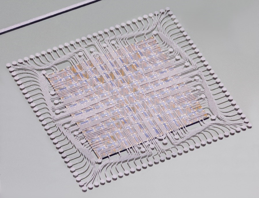
Here you can see a fully embedded chip with 220 interconnects and 20um line/spacing.
What are the technologies and materials you are working with?
We are working towards high throughput 3D Printed Electronics to enable this technology in volume manufacturing. At the moment, we have a custom stereolithography (SLA) 3D printer with our own control platform.
The 3D printer can pick and place components and add a wide range of conductive inks based on silver or copper particles. We are increasing the printer’s capabilities to provide higher resolution and more functional structures.
The SLA material used varies by application, ranging from stiff and temperature resistant to soft and flexible for robotics and sensor applications.
What are the advantages of 3D printing in your area?
We distinguish two main areas: printing electronic products and semiconductor packaging applications.
3D printing allows short lead times, printing shapes and geometry impossible with other manufacturing technologies for electronics products. For instance, an ECG sensor could be embedded in a wearable with electrodes positioned to precisely fit a wearer’s body.
For chip packaging, it is possible to create interconnects with a higher resolution with, for instance, wire bonding, while keeping all the flexibility of a digital system. Even for small series, it is possible to create custom packages combining multiple chips. Package footprints do not have to be determined by lead frames; with 3D printing, they are made directly. Compared to wafer-level packaging, the process involves fewer steps, making additive lithography significantly faster and cheaper.
What is your point of view on the future of 3D printing?
3D printing can be a standard production method for several different markets. It is the case for dental and jewelry applications where existing technologies are being replaced. We see the development of 3D Printed Electronics going in two main directions: low volume production of complex products and high volume chip packaging applications. 3D printing could also be an excellent manufacturing option to make semiconductors needing rapid innovation. Processes are improved and re-invented continuously to keep up with the yearly release of new devices.
As you can see, 3D printing can have many applications, from manufacturing electronics products to special chips and circuits. Choosing Additive Manufacturing and your manufacturing technology will help you develop your innovation processes to keep your time-to-market as efficient as possible for this competitive industry!