 Connect with Google
 Connect with Facebook
Conductive 3D printing: How can additive manufacturing help electronics?
Posted By Lucie Gaget on Sep 4, 2018 | 0 comments
Additive manufacturing can be really useful for electronics: you could totally use this 3D printing technology to manufacture the enclosure of electronic device, or to develop prototypes. Now, it is possible to go further and print the electrical elements. Indeed, a lot of devices are now 3D printable, but is it really possible to create conductive 3D printed objects?
In this blog post, we are going to see how additive manufacturing can help to create electrical systems and how conductive 3D printing is now becoming a reality.
How can 3D printing be useful for electronic?
The additive manufacturing technology is quite useful for electronic applications.
Some of our customers with electronic projects are for example using our 3D printing service to manufacture enclosures. Or, for example, Simusolar, one of our clients, is using 3D printing to manufacture parts of circuit boards. Read more about this amazing project here.

For your electronics project, 3D printing can be useful to develop prototypes, but also to produce. Indeed, if you need a prototyping solution, this method will allow you to make many iterations at a lower price and will be perfect to help you to develop your final product. Thanks to all the materials available on an online 3D printing service like Sculpteo, you will be able to produce qualitative parts.
Conductive 3D printing could allow going even further. The creation of electronic devices with conductive features using 3D printing can particularly be useful to develop IoT (Internet of Things) projects. It could be a way to develop even better and efficient products.
Conductive 3D printing: Offering new possibilities
Several experiments have been made to create conductive 3D printed parts. This innovation could allow you to create 3D printed devices like LED, or touch sensor. But it could be involved in bigger projects, in soft robotics, 3D electronics, and also for communication devices such as 3D printed Near Field Communication (NFC) antennas.
Let’s see what the viable possibilities to 3D print conductive devices are, using new 3D printing material or new printing techniques.
Conductive 3D printing materials
Graphene
There are some conductive materials that could totally revolutionize new electronic constructions. We already told you about graphene, the wonder material in 3D printing. This material has great intrinsic properties. Indeed, it is not only one of the most resistant materials, but it is also electrically conductive!
The structure of this material makes it electrically conductive. Graphene is the structural element of many forms of carbon. Carbon atoms are arranged in a honeycomb structure and there is a single free electron in each atom.
This way, the material can transmit currents through these free electrons. Conductive graphene filaments could be a great solution to create functional electrical elements. Keep in mind that this material is still less conductive than metals such as iron or copper.
ABS and PLA filaments
Some electrically conductive filaments have been developed using some ABS or PLA material, like graphene PLA filament. Regarding the strength of this material, it is more flexible than traditional PLA but has less layer adhesion.
For the moment, it seems that the only conductive 3D printing materials available are filaments, which can be used on desktop 3D printers. Soon, bigger professional 3D printers could be able to print with these electrically conductive materials but to begin with, these first options are offering great possibilities.
Indeed, these filaments could be useful in the development of wearable electronics, making it possible to create small electrical circuits.
Hydroprinting conductive patterns
Here is another 3D printing method to develop conductive parts: hydroprinting.
A paper in Advanced Materials Technologies published by Professor Shlomo Magdassi with some other researchers from The Hebrew University of Jerusalem and The Nanyang Technological University in Singapore, these researchers actually found a solution to 3D print conductive patterns. Using hydroprinting on a 3D printed part is allowing to manufacture a functional 3D printed conductive part. This process enables to print several layers circuits. It only requires repeating the same printing process for as many layers as needed.
If you need more information about this impressive innovation and more details about the printing process of these conductive parts, please check our previous blog post, we tell you all you need to know about hydroprinting and conductive patterns!

The stretchable and conductive 3D printing material
Combining elasticity and conductivity in one material isn’t easy, but 3D printing enabled researchers to develop totally new materials. Why are they important? Stretchable and conductive materials are particularly interesting for biological systems and artificial intelligence.
There have been a few ways developed to achieve soft, but conductive materials. One of them is to add plasticizers and flexible channels to polymers. This allows for creating soft areas. Electronic fillers or ionic electrolytes, which are incorporated in paths, are responsible for conductivity.
Zhouyue Lei and Peiyi Wu, researchers from Shanghai, recently published a study ‘’A highly transparent and ultra stretchable conductor with stable conductivity during large deformation’’. Their challenge was to test the conductivity of flexible materials, in some cases, in extreme environments. Were any developments made?
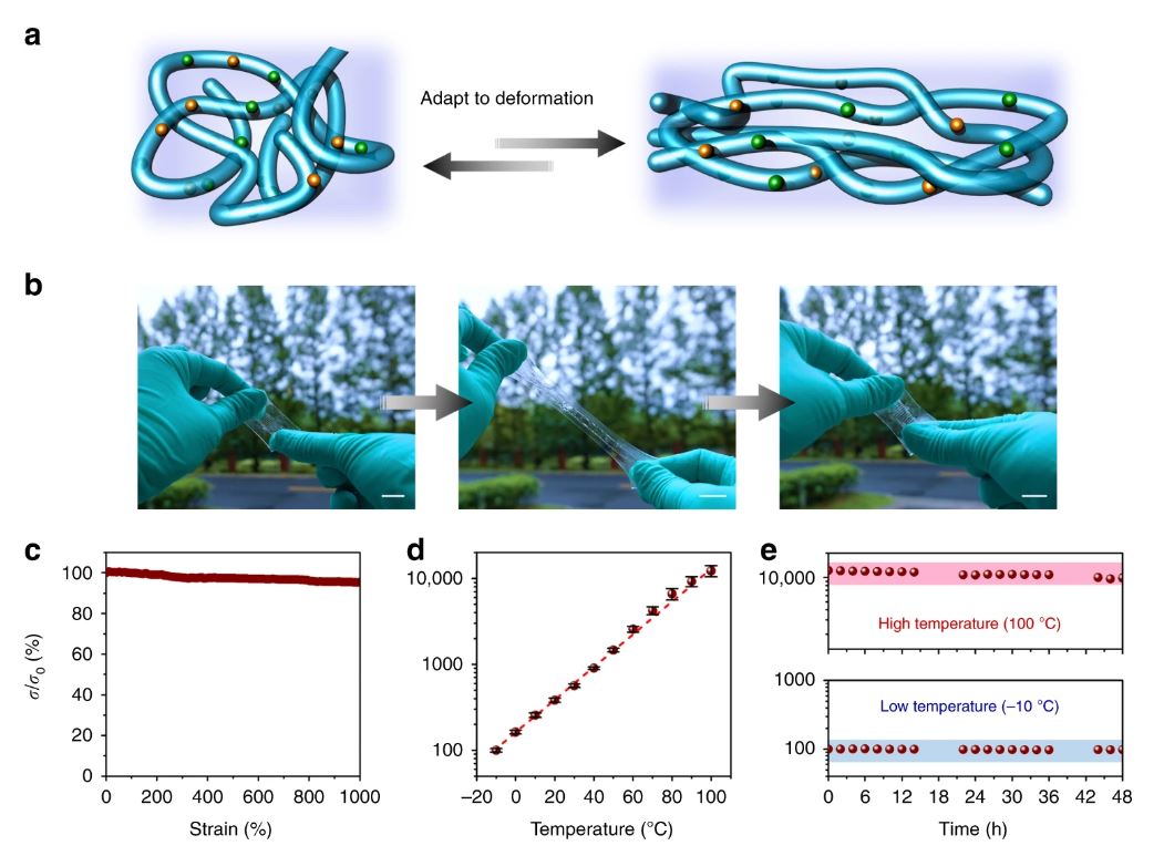
Electrical properties in dynamic environments. a Schematic illustration of the conductive paths in this material adapting to deformation. Blue lines represent ion nanochannels and the purple parts represent the dynamic networks. b Photographs of the 3D-printing conductor during a stretch-release cycle (scale bar: 2 cm). c The stability of the ionic conductivity during the deformation process. d The relative changes in ionic conductivity in the temperature range of −10 to 100 °C (error bars: standard deviations). e The stability of the ionic conductivity at extremely low or high temperatures for a long period. These measurements are humidity control (60 RH%)
https://www.nature.com/articles/s41467-019-11364-w
Lei and Wu studied transparent materials and their electromechanical characteristics, defects, and deformations. Their mission was to produce soft nanochannels, connected with crosslinked networks. The result was a 3D printing material, filled with conductors and paths which ‘’dynamically adapted’’ to stretching and deformation.
The authors comment: ‘’Herein, we introduce a type of intrinsically stretchable conductors. Small-molecular liquid-like electrolytes, such as ILs, provide charge carriers; polymers with similar ionic structures, e.g., polyzwitterions, realize ionic synergy with the liquid electrolytes and thus assemble conductive nanochannels to avoid aggregates or leaking risk of the electrolytes; dynamic networks are constructed by polymers that also have molecular synergy with the conductive nanochannels, to guarantee the structural integrity, deformation adaptability, and environmental stability.”
A great achievement was also prooving that the material kept its stability, performing a 3% chance of conductivity in 24 hours, and in extreme temperatures performed no melting point or glass transition.
This revolutionary development is very encouraging for the soft robotics industry. Without Additive Manufacturing technologies, the researchers wouldn’t be able to work in nanoscale, creating highly complex structures.
3D printing conductive elements in the future
All of the experiments made to create conductive systems using 3D printing technology are really promising. Nanotechnology and metal 3D printing could soon allow printing really small conductive components, circuit boards, and electrical circuits. Hydroprinting and new conductive materials are all offering to brand new possibilities and could make it possible to create fully 3D printed electronic devices.
As you can see additive manufacturing has a lot to offer for electronics. It could become quite common to 3D print electrical elements. If you have an electronic project, but you don’t know what software you could use to start it: here is our selection of the best CAD software for electronics. Then, don’t hesitate to try out our online 3D printing service. You will just have to upload your 3D file, we will take care of it and send you your 3D printed objects in a few days.
Don’t forget to subscribe to our weekly newsletter to learn about all the different 3D printing applications.